 © Fraunhofer CSP
Photovoltaics
Efficient solar cells developed from float-zone silicon
Higher efficiencies, for example more output for the same amount of solar irradiation, are the central development goals for new solar cells. In addition to the materials used, the life cycle costs are influenced by the individual components and ultimately the type of solar cell. In the KosmoS project, the scientists researched float zone crystals to produce more effective solar cells and investigated the use of thinner wires to cut more wafers from a silicon block. They were ultimately able to reduce the power generation costs of the entire photovoltaic system by 10 per cent compared to systems that use conventional silicon solar cells (Al-BSF solar cells, short for: aluminium back-surface-field) with screen-printed aluminium paste on the rear side.
Project context
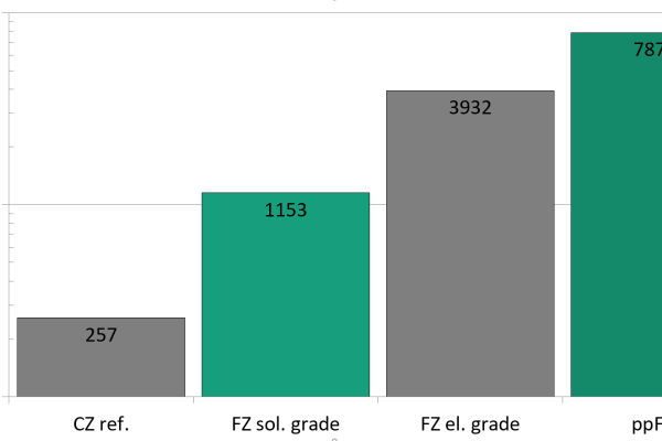
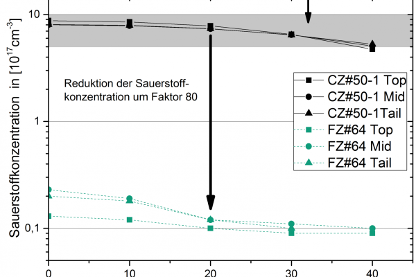
So-called float zone silicon is suitable as a raw material for particularly efficient n-type solar cells that have negative base doping, i.e. an excess of electrons. This has less contamination and an oxygen concentration that is 100 times lower. Consequently, the output of solar cells increases and the efficiency of the entire photovoltaic system can be improved. Despite these advantages, crystals made of float zone silicon have been little used to date. Compared to the usual Czochralski method, the complex production of the crystals is more costly.
Research focus
Within the project KosmoS: short for "cost-optimised high-efficiency solar cells made of low-oxygen n-type mono-silicon for industrial mass production", the scientists investigated the silicon raw material along the value chain up to the solar cell. They used float zone silicon for their new concept of a rear side solar cell. This high-quality material is suitable for exploiting the potential of this new n-type solar cell and surpassing the efficiency of bifacial monocrystalline PERC cells and nPERT cells. Both of these types are solar cells that absorb light from both sides.
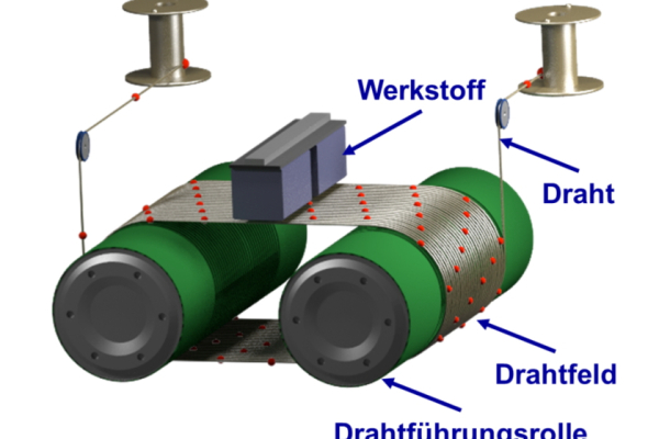
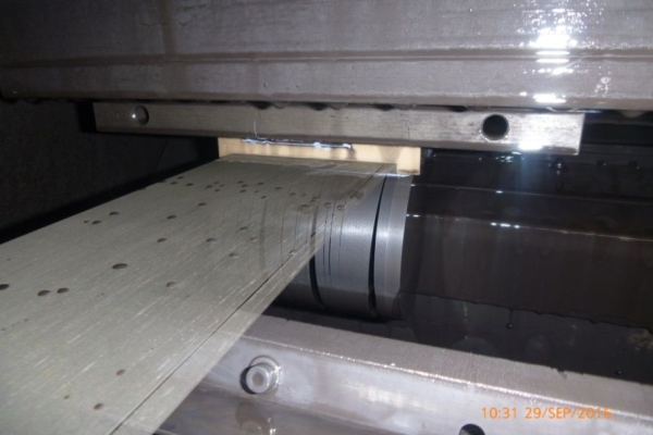
Solar cells consist of thin silicon slices, the wafers. These are cut from the silicon crystals in special procedures using wire saws. Multiple wire loops cut the crystal block in one sawing step. Thinner wires save material and costs. The researchers therefore investigated the procedure and tested the use of finer wires.
Innovation
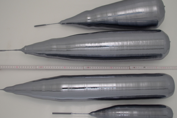
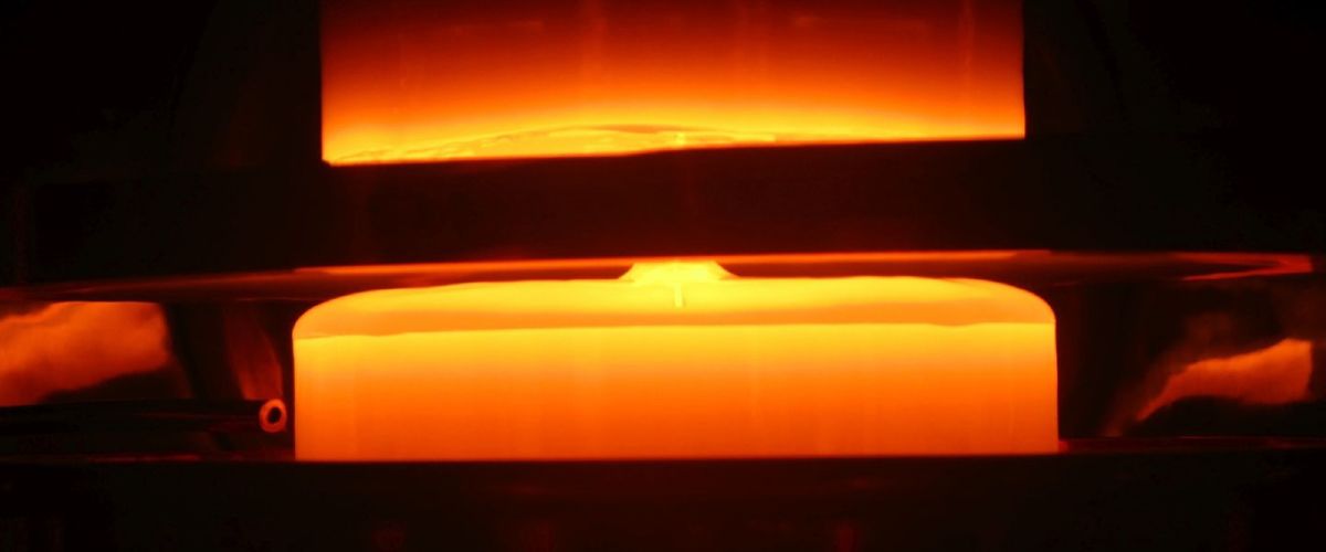
High-purity float zone silicon crystals are produced from stocks of silicon rods. The scientists at the Fraunhofer CSP have developed a cost-effective method to produce these rods - the pre-pulling float zone process.
In the production of solar cells, lasers are used as tools to open the dielectric layers of the solar cell. This can cause damage to the contacts of the solar cells, which can now be determined using a new method. For this purpose, the scientists at the ISC Konstanz have developed an analytical method known as photoluminescence spectroscopy. This enables them to describe not only the damage caused by laser processing but also the recombination of metal contacts applied by screen printing.
Results
Within the project, the researchers have developed highly efficient n-PERT back junction solar cells. These bifacial solar cells show a high efficiency of more than 21.6 per cent and have 10 per cent lower power generation costs in the PV system compared to conventional solar cells (Al-BSF solar cells). Their structure and process is similar to the pPERT cell; the substrate, boron emitter and its passivation correspond to the n-PERT cell.
More wafers from one silicon crystal reduce costs
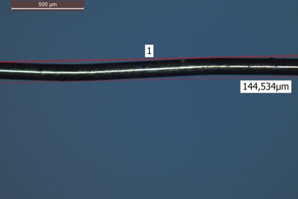
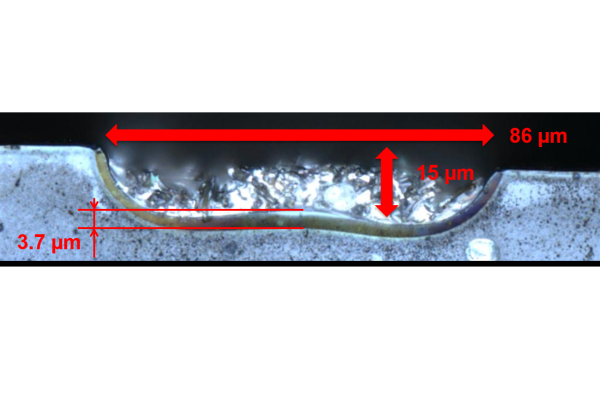
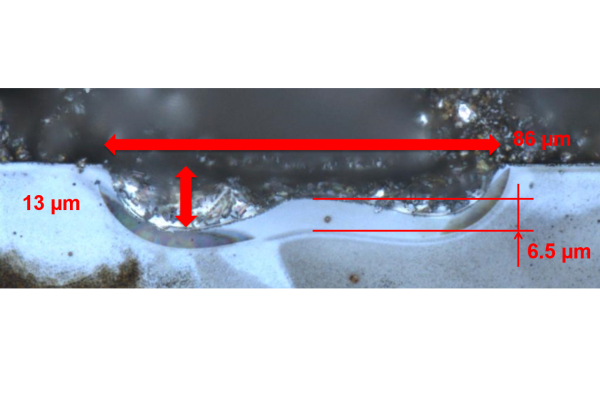
The scientists investigated the multi-wire sawing process with structured wires and cut wafers from monocrystalline float-zone crystals. The aim was to use very thin wires with a diameter of 115 to 100 micrometres so that more wafers could be sawed from one crystal. They achieved good results with 105 micrometre thin wires and have further developed the method to production maturity. Compared to the 120 micrometre thick wires currently in use, the new method saves 15 micrometres of material per saw cut. This allows 5 per cent more wafers to be cut per millimetre of block length.
Practical transfer
ISC Konstanz is continuously refining the bifacial n-PERT Back Junction solar cells and offers the manufacturing process for licensing. RCT Solutions will incorporate the n-PERT Back Junction solar cells into a new production line as part of its technology solutions.

